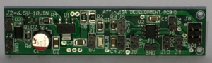
ATtiny13A Development PCB
….Full Technical Information
- Development / Breakout PCB for ATtiny13A MCUs – Compatible with ATtiny13 and ATtiny13A (ships with ATtiny13A)
- Control up to 5 I/O ports – using software written in C or Assembly code
- SPI programming port – to connect programming interface (use ATMEL Studio 7 to upload programs to the ATtiny13A development PCB
- 6.5V to 18V power input (D.C.)
- 5V MCU I/O levels (‘U1’ regulator can be changed for 3.3V MCU I/O levels if required)
- 1206 (imperial size) surface mount components
- Quality components used (Taiyo Yuden, Wurth Electronics, Amphenol FCI, Yageo, ON Semiconductor, Diodes Incorporated, ATMEL)
- Gold plated 0.1″ pitch headers – for long life, two pins per connection / port for easy connection
Complete Technical Description
PCB Dimensions
2.83″ length x 0.67″ width
PCB 1.6mm (63 mil) thickness
Package Dimensions (shipped)
Package Weight (shipped)
ATtiny13A Core
The heart of the PCB is the ATtiny13A MCU, which can be programmed via the on-board SPI header using ‘ATMEL JTAG ICE3’, ‘ATMEL ICE for AVR’ programming interfaces (or similar) via a 6-pin SPI header…
The MCU’s details are given below…
The ATtiny13A device can be programmed using ATMEL Studio 7 using C or Assembly code to control up to 5 I/O ports (see ATtiny13A data sheet for full details of the ATtiny13A pins and available functions – ADCs, PWM, etc…).
Note that nRST (RESET pin 1, PB5) should be programmed as INPUT, so programming interface can reset the ATtiny13A device during programming)!!
The ATtiny13 and ATtiny13A are the same MCU, but the ATtiny13A uses ‘pico power’ giving a low power MCU.
Power OK LED
LED1 is a GREEN 5V power OK LED indicator and draws 20mA from the 5V rail.
Power, Ground and I/O Connections – Headers
All headers are gold plated 0.1″ type headers – for long life.
Each connection has two pins available for easy connection / prototyping.
Powering the MCU directly
The MCU can be powered directly using header connection ‘J1’, if component ‘R1’ is removed.
‘J1’ (normally a 5V output from ‘U1’) can be used to apply a 1.8V to 5V voltage, to run the MCU directly…
Note, with the PCB used in this mode, ‘R1’ must be removed to prevent damage to ‘U1’.
The green ‘Power OK’ LED (LED1) will still light for any voltage greater than around 3V applied at the ‘5V’ output (with ‘R1’ removed!!)
Connecting / Programming the PCB
The PCB works from a 6.5V to 18V DC power input.
-
Positive input power voltage is applied at either pin of ‘J2’.
-
Ground input power voltage is applied at either pin of ‘J3’
An SPI programming port is used to write software into the AT13 MCU.
A programming device such as the ‘ATMEL JTAGICE3’ or ‘ATMEL ICE for AVR’ can be connected directly to ‘J8’ programming port (6-pin SPI).
Frequently Asked Questions (FAQs)…